TESCAN ORSAY HOLDING a.s. has announced the revolutionary new TENSOR – the first 4D-scanning transmission electron microscope (4D-STEM) built from the ground up for a totally new level of performance and user experience. TENSOR is designed to address the needs of anyone with an interest in multimodal nano-characterization applications (morphological, chemical, and structural), including materials scientists, semiconductor R&D and failure analysis (FA) engineers, and crystallographers.

“With the launch of TENSOR, TESCAN is the go-to company for turnkey ‘medium-voltage’, Schottky FEG, analytical 4D-STEM solutions,” said Jaroslav Klíma, Chief Executive Officer of TESCAN ORSAY Holding (TOH a.s.). “TESCAN understands the challenges of integrating not only STEM, but 4D-STEM capabilities particularly, onto legacy TEM columns. This extensive knowledge was leveraged into the design, from the ground up, whereby scanning of the electron beam is synchronized with diffraction imaging using a hybrid-pixel direct electron detector, electron beam precession, EDS acquisition, beam blanking, and near real-time analysis and processing of 4D-STEM data.”
JK Weiss, TEM Applications R&D Manager and General Manager of TESCAN Tempe, adds, “It is not just the hardware that sets this system apart from every other TEM currently available on the market, but rather, it’s the integration of the hardware and software for a totally revolutionized new user experience that does not require months of Ph.D. or post-doc training or hours of column adjustments between different analysis modes.”
For materials scientists and semiconductor R&D and FA engineers, the TENSOR 4D-STEM provides multimodal, high contrast, high-resolution 2D & 3D characterization of functional (engineered) materials at the nanoscale:
➤ STEM imaging (bright field, annular dark field, high-angle annular dark field)
➤ STEM lattice imaging
➤ Composition (quantitative EDS and elemental mapping)
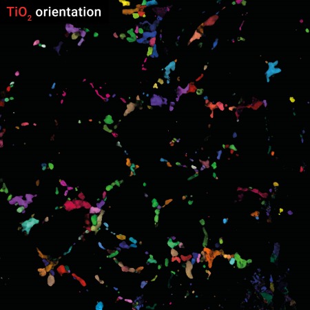
➤ Orientation and phase mapping
➤ Strain mapping
➤ Virtual STEM and data export
➤ STEM, STEM-EDS, and diffraction tomography
Applications within the semiconductor lab include multimodal nano-characterization of thin films for R&D and failure analysis of logic, memory, and storage devices and advanced packaging.
For crystallographers, the TENSOR STEM helps to determine the crystallographic structure of small, sub-micron natural or synthetic particles that are too small to be characterized using micro-XRD techniques.
“TESCAN TENSOR is the next example of innovation by TESCAN, following the company’s launch of the world’s first focused ion beam/scanning electron microscope (FIB/SEM) and Plasma FIB/SEM, time-of-flight secondary ion mass spectrometry (ToF-SIMS) applications on FIB/SEM platforms, Dynamic-CT and Spectral-CT,” said Vratislav Koštál, Chief Product Officer at TESCAN. “We’ve listened to our customers and delivered what they’ve asked for―a more accessible TEM solution that is high-performing and productive for mainstream use.”
For more information: www.tescan.com
Tags: 3d vina, hiệu chuẩn, hiệu chuẩn thiết bị, máy đo 2d, máy đo 3d, máy đo cmm, New TENSOR Scanning Transmission Electron Microscope Unveiled, sửa máy đo 2d, sửa máy đo 3d, sửa máy đo cmm
