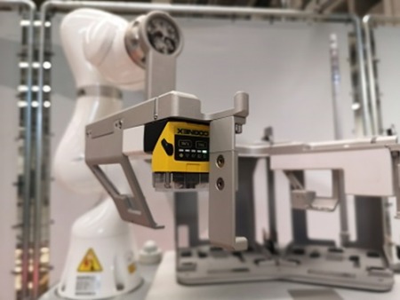
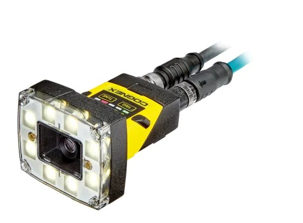
With the Semi Mobility Solution, KUKA has taken a decisive step in semiconductor production automation. Until recently, robotics have been used in the individual production steps. Kuka has created a mobile robot that is also responsible for transporting the highly sensitive wafers from station to station. On board the robot is an image processing system from Cognex that is high-performing, yet compact in size.
 Semiconductors’ performance dictates the pace of innovation. This applies just as much to industrial automation as to digital communication via cell phones, laptops, smart building technology, and the automobile industry. And the market is continuing to grow. In 2018, the international semiconductor industry achieved $481 billion in sales revenue and this figure is set to reach $525 billion as early as 2022 according to a study by PwC.
The robotics industry is also taking advantage of this trend, as, for example, the latest generation of controls and controllers offer additional functions. Conversely, however, the innovative capacity of robot manufacturers is also accelerating the efficiency and productivity of microprocessor manufacturers. KUKA offers a wide range of extremely flexible robots that can also be quickly tailored to a whole variety of handling requirements, as the life cycle of semiconductors is short and the market correspondingly volatile.
Mobile Handling System for Cleanrooms
Using robotics, individual production steps can be automated effectively and to a high-quality standard. However, up until now, robotics have not been used to transporting semiconductor substrates (wafers) from one workstation to the next. Ideally, semi-conductor manufacturers would prefer end-to-end automation, because pristine cleanroom conditions can be much better achieved with ‘unmanned production’. Until now, however, this aspect of the process was untenable due to the lack of precision with which mobile robots move and grasp.
KUKA has now developed the world’s first single-source solution for the automated transport and handling of semiconductor cassettes: the ‘Semi Mobility Solution’. In this instance, a lightweight LBR iiwa robot is mounted on a KMR 200 CR autonomous automated guided vehicle (AGV). The AGV can manoeuvre in the smallest of spaces and KUKA’s engineers have developed a sophisticated gripper system for the handling.
 System solution: AGV plus Robot Arm plus Gripper
The Semi Mobility Solution goes to a handover point where wafer transport boxes are located. When the AGV has reached its destination, the robot arm is in place to precisely determine its position with the help of an integrated image processing sensor and performs a fine calibration.
This moves the robot into the position to grasp the transport box with a high degree of accuracy and deposit the sensitive wafers without any vibrations in a storage space on the AGV platform. Using this approach, the robot can pick up and transport two different sizes of boxes for wafers with a diameter of 200 or 300 mm. Once it has reached its destination, the robot delivers the transport boxes on the respective processing line.
The Semi Mobility Solution moves around the room on the basis of stored destinations but chooses the route there itself. The navigational capacity of the LBR iiwa platform enables it to move autonomously in a safe and sensitive way. Environment tracking is supported by laser scanners. They perceive the environment in real time, thus preventing collisions.
For more information: www.cognex.com
Tags: 3d vina, hiệu chuẩn, hiệu chuẩn thiết bị, Image Processing Guides Mobile Robot Gripping Process, máy đo 2d, máy đo 3d, máy đo cmm, sửa máy đo 2d, sửa máy đo 3d, sửa máy đo cmm