The most sensitive and high precision optical systems are made possible by the ability to produce optics with — in some instances — sub-angstrom surface roughness. The polishing processes that allow such smooth optics are enabling technologies that lead to the creation of cutting-edge and innovative end-use products. These optics are extremely demanding to fabricate, and also push metrology tools used to verify surface roughness to their limits.
Many polishing techniques can be used to manufacture high-quality optical surfaces, ranging from surface generation, grinding, lapping and full-aperture pitch polishing, to more advanced techniques such as deterministic figuring using MRF (magnetorheological finishing), ion beam figuring, and computer-controlled polishing. Specialized processes such as diamond turning and polishing are also used for some applications.
Each process has one thing in common – they remove a certain amount of material from the optic being polished. But beyond this, each leaves behind a unique signature of the process itself, a “fingerprint” that can affect the performance of the final optical system in a variety of ways, most typically leading to variations in optimal imaging or light scattering.
To ensure the polished optic meets the requirement of a particular application, it is vital that the polishing process used to make a surface is understood and characterized. This article looks at one such powerful characterization tool, a 3D optical profiler using coherence scanning interferometry (CSI).
Coherence Scanning Interferometry
At the heart of the CSI profiling technology are specialized optical microscope objectives that not only provide the imaging and magnification of a surface, but also measure the 3D topography of that surface (Figure 1). The microscope’s illuminator projects light through the objective, where a beam-splitter sends some of the light to the reference mirror and some to the part under test.
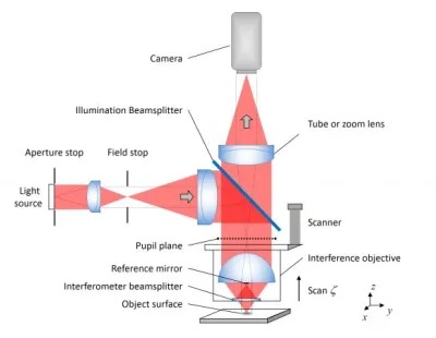
When the optical path length from the beam-splitter to both the reference and test surfaces is equal, the reflected light from both the surfaces recombines, and this results in interference “fringes” at the detector. The shape and position of these fringes are directly proportional to the difference in height between the test surface and the reference mirror.
Effectively, therefore, the fringe shapes produced can be thought of as contours of the surface being measured, where the contour intervals are proportional to the illumination wavelength. Processing algorithms can further refine the precision of the technology to small fractions of the wavelength.
To profile the test surface’s topography, the microscope objective is scanned perpendicular to the test surface. A camera and computer system monitor the changing fringe patterns during the scan, and sophisticated algorithms interpret these patterns to construct a 3D map of the surface. Using this technique, surface topography measurements at the sub-nanometer level can routinely be made over any field of view, usually in anything from 5-20 seconds. With appropriate measurement averaging and careful attention to the vibration and noise conditions in the metrology area, the same equipment can yield sub-angstrom measurements.
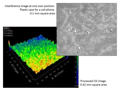
CSI profiling is completely non-contact, which eliminates any chance of the sample being tested being damaged in any way. Also, in contrast with other microscope-based 3D topography techniques, CSI has the distinct advantage that the height resolution of the measurement is consistent across all magnifications, whether the field of view is 20μm or 20mm. (Figure 2.)
Fingerprints
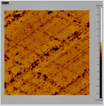
When making high quality optics, early in the manufacturing process, raw glass is roughly generated and then ground using various sizes of abrasive materials to reach a nominal shape. At this stage, the surface of the optic being manufactured is typically very rough and diffuse, and an CSI profiler can highlight the directional nature of the grinding media and unremoved pits and spikes that form as a result of these operations. In order to keep the manufacturing process as short as possible, it is important to minimize the presence and magnitude of these marks. ( Figure 3)
The polishing methods used to complete a finished optic vary widely in the way that they remove material and in the characteristics of the surface when it is complete. With the surface texture in-turn having a profound effect on the efficiency and light-scattering characteristics of the final surface, it is extremely important to be able to predict the outputs of each process.
In traditional precision optics manufacturing, two key polishing processes are employed, pitch laps and polishing pads. Other deterministic approaches include magneto-rheological finishing (MRF) and ion-beam figuring (IBF), which can locally and precisely remove material. For this investigation, however, we’ll consider the first two. Pitch laps are commonly used when the requirement is for ultra-precise optics, pitch produced as a consequence of the distillation of tar derived from wood or petroleum. Compared to the glass that it is used to polish, pitch is very soft, and because of this it will not scratch the optic being worked. The viscosity of pitch also means that it can slowly flow at room temperature, and this in turn allows it to mould to the shape of the optic being polished and remain in close contact.
Pitch laps provide exceptional performance, but they are labor intensive, and require significant maintenance and attention at change over. Because of this, many production parts today are polished using laps faced with polishing pads made of polyurethane, which are very stable, and polish more quickly than pitch as they can run at higher pressures and speeds. They don’t “flow” like pitch, however, and they do not conform well to the shape of the optic. Because of this, they will work on a narrower range of surfaces.
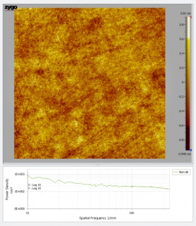
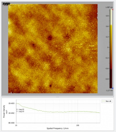
Figure 4a shows some of the different surface characteristics that can be seen when different polishing methods are chosen. The surface of the pad-polished sapphire surface in Figure 4 shows a rolling surface with significant low-frequency waviness. The surface of the fused silica optic — polished using traditional pitch methods — is characterized by a more uniform texture. (Figure 4b)
The chosen polishing technique will ultimately be determined by the final application of the surface being manufactured, but it is vital that tools are available to assess the differences in the processes employed in order quantify surface texture to best fit to the end-use application.
Quantifying Surface Texture
There are a number of ways that the surface texture of an optic can be quantified.
Sa and Sq. Perhaps the easiest and most common way of quantifying surface texture is through a root mean square (Sq) or average roughness (Sa) parameter. While a good starting point, Sq and Sa, however, only give a partial view when measuring a surface. For example, we have seen that different polishing processes can produce completely different surfaces visually, but they can show identical Sq and Sa values. This can easily be seen in the surface map images from Figures 4, both of which have an Sa of 0.22 nm.
Power Spectral Density (PSD) Plot. One very powerful tool in assessing optical surface condition is the power spectral density (PSD) plot. PSD plots use Fourier processing to reduce a surface to frequencies with a certain magnitude. Regular features in the surface will appear as spikes at a specific frequency and correspond to different surface treatment methods.
Every surface map can be considered a summation of sine waves with varying amplitude. The PSD uses a Fourier analysis (a method of defining periodic waveforms in terms of trigonometric functions) to reduce the surface map into these sine waves. The power (the square of the amplitude) of the component waves is plotted as a function of the frequency. This enables quantitative identification of frequency-dependent process signatures that cannot be seen with simpler roughness analysis.
The same PSD analysis can be specified across a wide range of spatial frequencies with large-scale form and waviness data from large-aperture figure interferometers, through CSI profilers, and even down to the finest lateral scale atomic force microscope.
Once again, the images in Figure 4 a and b show two polished surfaces with clearly different surface morphology, measured on a ZYGO NewView CSI profiler. These two surfaces have the same average roughness value (0.2 nm Sa), but careful analysis of the PSD plots below each shows meaningful differences. The sapphire surface, with its roughness content dominated by lower-frequency waviness, has more energy on the left side of the PSD and then drops off quickly between 10 to 30 cycles per mm. The fused silica, however, is more uniform, with its roughness dropping linearly from 10 to 30 cycles per mm.
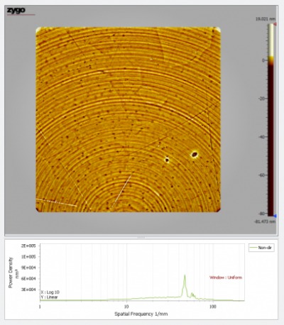
Another example of a surface where PSD is useful is shown in Figure 5, which is a diamond-turned optical surface with a clear, grooved structure that results from the single-point diamond-turning process. The PSD shows the frequency of this structure as a peak at 45 cycles per mm. A surface such as this is often perfectly acceptable for IR applications, but would be completely unacceptable for most visible and UV applications due to significant scattering and imaging degradation which would result.
For more information: www.zygo.com
Tags: 3d vina, hiệu chuẩn, hiệu chuẩn thiết bị, High Quality Optical Surfaces — Characterizing The Polishing Process Fingerprint, máy đo 2d, máy đo 3d, máy đo cmm, sửa máy đo 2d, sửa máy đo 3d, sửa máy đo cmm
